Login or Register for FREE!
Subelement E6
CIRCUIT COMPONENTS
Section E6A
Semiconductor materials and devices: semiconductor materials; germanium, silicon, P-type, N-type; transistor types: NPN, PNP, junction, field-effect transistors: enhancement mode; depletion mode; MOS; CMOS; N-channel; P-channel
In what application is gallium arsenide used as a semiconductor material in preference to germanium or silicon?
  • In high-current rectifier circuits
  • In high-power audio circuits
  • Correct Answer
    At microwave frequencies
  • At very low frequency RF circuits

Gallium Arsenide (GaAs) semiconductors really shine at higher frequencies. They have less noise as compared to silicon, reduced sensitivity to heating, higher electron mobility, and higher saturated electron velocity. This makes them usable for frequencies up to 250GHz.

Unrelated Memory Trick: The genus of chickens is "Gallus", so just think Gallium is microwaved chicken.

Last edited by midden. Register to edit

Tags: none

Which of the following semiconductor materials contains excess free electrons?
  • Correct Answer
    N-type
  • P-type
  • Bipolar
  • Insulated gate

N-Type material contains an excess of free electrons. Electrons hold a negative charge, so think of "N-Type" as "Negative" as a way to remember.

Last edited by orochimaru. Register to edit

Tags: none

What are the majority charge carriers in P-type semiconductor material?
  • Free neutrons
  • Free protons
  • Correct Answer
    Holes
  • Free electrons

Avoid the temptation to assume that P-type uses protons as its majority charge carrier -- it does not!!

Instead, P-Type material is like a hotel with lots of vacancies for electrons. These vacancies are "holes".

Last edited by orochimaru.

Visualization tip: Imagine the "hole" (white space) in the middle of the letter 'P'.

Or just remember: "N: no holes, P: potholes"

Last edited by ericthughes. Register to edit

Tags: none

What is the name given to an impurity atom that adds holes to a semiconductor crystal structure?
  • Insulator impurity
  • N-type impurity
  • Correct Answer
    Acceptor impurity
  • Donor impurity

The correct answer is Acceptor impurity, because an acceptor impurity creates holes in the semiconductor crystal lattice where electrons could fit.

A donor impurity is incorrect as it would add extra electrons to the semiconductor crystal. An N-type impurity would also be incorrect, because this is another way of describing a donor impurity.

There's no such thing as an insulator impurity, so that one is a pure distractor.

Remember: aCCeptors "aDD" holes while Donors "provide" electrons.

Last edited by dornierpilot. Register to edit

Tags: none

What is the alpha of a bipolar junction transistor?
  • The change of collector current with respect to base current
  • The change of base current with respect to collector current
  • Correct Answer
    The change of collector current with respect to emitter current
  • The change of collector current with respect to gate current

The "alpha," or \(\alpha\) is the ratio of the collector current to the emitter current.

\[\alpha = \frac{I_{\text{collector}}}{I_{\text{emitter}}}\]

Equation 5-2, pg 5-9 ARRL Extra Class License Manual.

So the answer is: The change of collector current with respect to emitter current.


Hint: ACE, Alpha = Collector over Emitter...

Last edited by wileyj2956. Register to edit

Tags: none

What is the beta of a bipolar junction transistor?
  • The frequency at which the current gain is reduced to 1
  • Correct Answer
    The change in collector current with respect to base current
  • The breakdown voltage of the base to collector junction
  • The switching speed of the transistor

The Beta of a transistor is a published ratio of the change in collector current that results from a change in base current. A typical value for a small transistor is 100-150, while "high gain" transistors may have higher beta values. Power transistors, on the other hand, tend to have a lower value of beta. Beta is also called the "common emitter current gain."

It is widely considered bad practice to design a transistor circuit that is dependent on beta for biasing or proper function. For a bipolar junction transistor, beta changes as a function of temperature. Unfortunately, it increases which can lead to a condition known as "thermal runaway".


A mathematical identity is given in Wikipedia:

\[\beta=\frac{I_C}{I_B}=\frac{\text{collector current}}{\text{base current}}\]

This is roughly representative of the correct answer in which the beta, or \(\beta\), is the change in collector current with respect to the base current.

SILLY HINT: What is the fate of a bipolar disfunction transition? - Change in current mood with respect to base mood.

Last edited by yr7 - extra. Register to edit

Tags: none

In Figure E6-1, what is the schematic symbol for a PNP transistor?
  • Correct Answer
    1
  • 2
  • 4
  • 5

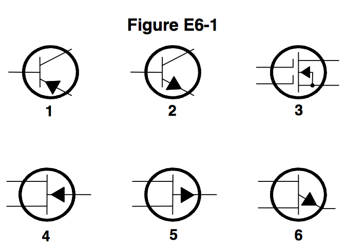
A nmemonic device to remember BJT transistors is: NPN = Not Point iN PNP is the opposite.


My 2 cents mnemonic.

P = Positive = comes IN N = Negative = comes OUT.

You need to remember that PNP or NPN apply to EBC: Emitter, Base, Collector and the Collector is the one with the triangle.

PNP would then be: Emiter : P = comes in Base: N = comes out Collector: P = comes in

So we are looking for a Transistor (1 or 2) and the only one with "comes in" at the collector is the first choice (#1).

Last edited by chevdor. Register to edit

Tags: none

What term indicates the frequency at which the grounded-base current gain of a transistor has decreased to 0.7 of the gain obtainable at 1 kHz?
  • Corner frequency
  • Alpha rejection frequency
  • Beta cutoff frequency
  • Correct Answer
    Alpha cutoff frequency

The performance of a transistor amplifier is relatively constant up to a point. When the frequency exceeds this point, the performance of the transistor degrades as frequency increases. The Beta Cutoff Frequency is the frequency at which the current gain falls to unity. The Alpha Cutoff Frequency is the frequency at which the current gain falls to 0.707 of the low frequency current gain.

Last edited by kd7bbc. Register to edit

Tags: none

What is a depletion-mode FET?
  • Correct Answer
    An FET that exhibits a current flow between source and drain when no gate voltage is applied
  • An FET that has no current flow between source and drain when no gate voltage is applied
  • Any FET without a channel
  • Any FET for which holes are the majority carriers

There are essentially two flavors of field-effect transistors (FETs):

  • enhancement mode
  • depletion mode.

Most Junction FETs (JFET, or just FET) are depletion mode, while most many MOSFETS are enhancement mode devices.

Depletion mode FETs will exhibit "normally on" behavior. That is to say that current will flow between the source and drain even when the voltage between the gate and the source (\(V_\text{gs}\)) is zero.

To stop the flow of current you need to "deplete" the gate -- pull it below the device's specific threshold voltage

HINT: "When the going gets tough, the tough get going." (You can relate this to "depletion" & "current")

(\(V_\text{th}\)). When \(V_\text{gs} < V_\text{th}\), the gate is "depleted" and current flow will stop.

Last edited by yr7 - extra. Register to edit

Tags: none

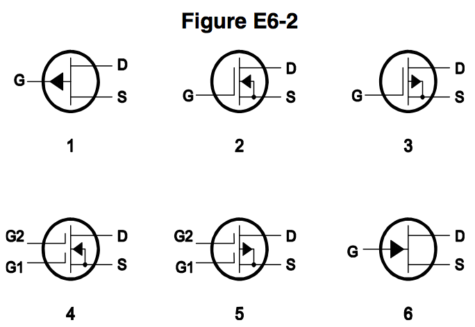
In Figure E6-2, what is the schematic symbol for an N-channel dual-gate MOSFET?
  • 2
  • Correct Answer
    4
  • 5
  • 6
This question does not yet have an explanation! Register to add one

Tags: none

In Figure E6-2, what is the schematic symbol for a P-channel junction FET?
  • Correct Answer
    1
  • 2
  • 3
  • 6

Hint: There are only two symbols from this list of six possible on the exam, #1 and #4. Both have an arrow pointing toward the gate (G) or gates (G1 & G2) on the left side of the symbol. "The N-channel does Not have two gates."

Symbol 1 is the P channel junction FET (field-effect transistor) which is also called a MOSFET (metal-oxide semiconductor field-effect transistor).

Last edited by taco40. Register to edit

Tags: none

Why do many MOSFET devices have internally connected Zener diodes on the gates?
  • To provide a voltage reference for the correct amount of reverse-bias gate voltage
  • To protect the substrate from excessive voltages
  • To keep the gate voltage within specifications and prevent the device from overheating
  • Correct Answer
    To reduce the chance of the gate insulation being punctured by static discharges or excessive voltages
This question does not yet have an explanation! Register to add one

Tags: none

What do the initials CMOS stand for?
  • Common Mode Oscillating System
  • Complementary Mica-Oxide Silicon
  • Correct Answer
    Complementary Metal-Oxide Semiconductor
  • Common Mode Organic Silicon

Complementary metal–oxide–semiconductor (CMOS) is a technology for constructing integrated circuits. CMOS technology is used in microprocessors, microcontrollers, static RAM, and other digital logic circuits.

CMOS is also sometimes referred to as complementary-symmetry metal–oxide–semiconductor. The words "complementary-symmetry" refer to the fact that the typical design style with CMOS uses complementary and symmetrical pairs of p-type and n-type metal oxide semiconductor field effect transistors (MOSFETs) for logic functions.

Two important characteristics of CMOS devices are high noise immunity and low static power consumption.

/wiki/CMOS

Hint: It's the only choice with the word semiconductor ;)

Last edited by sympathique. Register to edit

Tags: none

How does DC input impedance at the gate of a field-effect transistor compare with the DC input impedance of a bipolar transistor?
  • They are both low impedance
  • An FET has low input impedance; a bipolar transistor has high input impedance
  • Correct Answer
    An FET has high input impedance; a bipolar transistor has low input impedance
  • They are both high impedance

The base-emitter junction of a bipolar transistor draws a small, but non-zero amount of current. This lowers the effective input impedance of a bipolar transistor circuit.

Field-effect transistors (FETs) on the other hand, are essentially charge-based devices. While an ideal FET draws no current, real FET circuits draw minuscule amounts of current. This drives up in the input impedance significantly, making FET's ideal for applications where high input impedance is required.


Memory trick: bipolar >>> low; therefore FET must have high impedance.

Alternate memory trick: A fete (FET) is a celebration, think high spirits.

Best memory trick ever: Boba FET's jetpack enables him to fly higher.

HINT: FET trumps DC

Last edited by yr7 - extra. Register to edit

Tags: none

Which of the following semiconductor materials contains an excess of holes in the outer shell of electrons?
  • N-type
  • Correct Answer
    P-type
  • Superconductor-type
  • Bipolar-type

Refer to the link:

http://www.pveducation.org/pvcdrom/pn-junction/doping

P-type semiconductor material only has 3 valence electroncs, while N-Type has 5. An easy way to remember this is:

N = No Holes while P = Potholes.


Another way is to remember that the charge of electrons is negative https://en.wikipedia.org/wiki/Electron. The electron symbol is e-

If there are more holes, there are less electrons. If there are less "-", there are more "+".

Last edited by chevdor. Register to edit

Tags: none

What are the majority charge carriers in N-type semiconductor material?
  • Holes
  • Correct Answer
    Free electrons
  • Free protons
  • Free neutrons

Protons and Neutrons are stuck in the nucleus of an atom, do not move, so they can not be charge carriers.

Holes and Free electrons are our only two choices left.

There's two types of semiconductor materials. N-type and P-type.

N-type is named because the charge carrier is negative, which is the electron.

P-type is named because the charge carrier is positive, this is called a hole.

Last edited by sverasch. Register to edit

Tags: none

What are the names of the three terminals of a field-effect transistor?
  • Gate 1, gate 2, drain
  • Emitter, base, collector
  • Emitter, base 1, base 2
  • Correct Answer
    Gate, drain, source

The gate, drain, and source are the three terminals of a field-effect transistor.

The emitter, base, and collector are the three terminals of a bipolar junction transistor.

Memory aid: think fields (pastures) need gates.

Last edited by verticalham. Register to edit

Tags: none

Go to E5D Go to E6B