PRACTICAL CIRCUITS
Power supplies; and schematic symbols
What safety feature does a power-supply bleeder resistor provide?
-
It acts as a fuse for excess voltage
-
Correct AnswerIt discharges the filter capacitors
-
It removes shock hazards from the induction coils
-
It eliminates ground-loop current
Hint: a Bleeder causes a Discharge blood
The bleeder resister of a power supply performs the safety feature of discharging the filter capacitors. The resistor is arranged in parallel with the power supply. The use of the resistor is very important in this application, as it lowers the risk of electric shock from stored electrical energy in the filter capacitors by allowing the voltage level to decay quickly when the power supply is shut off.
For more info see Wikipedia: Bleeder resistor
The bleeder resistor is shown as symbol 9 on the G7-1 schematic for the general class exam.
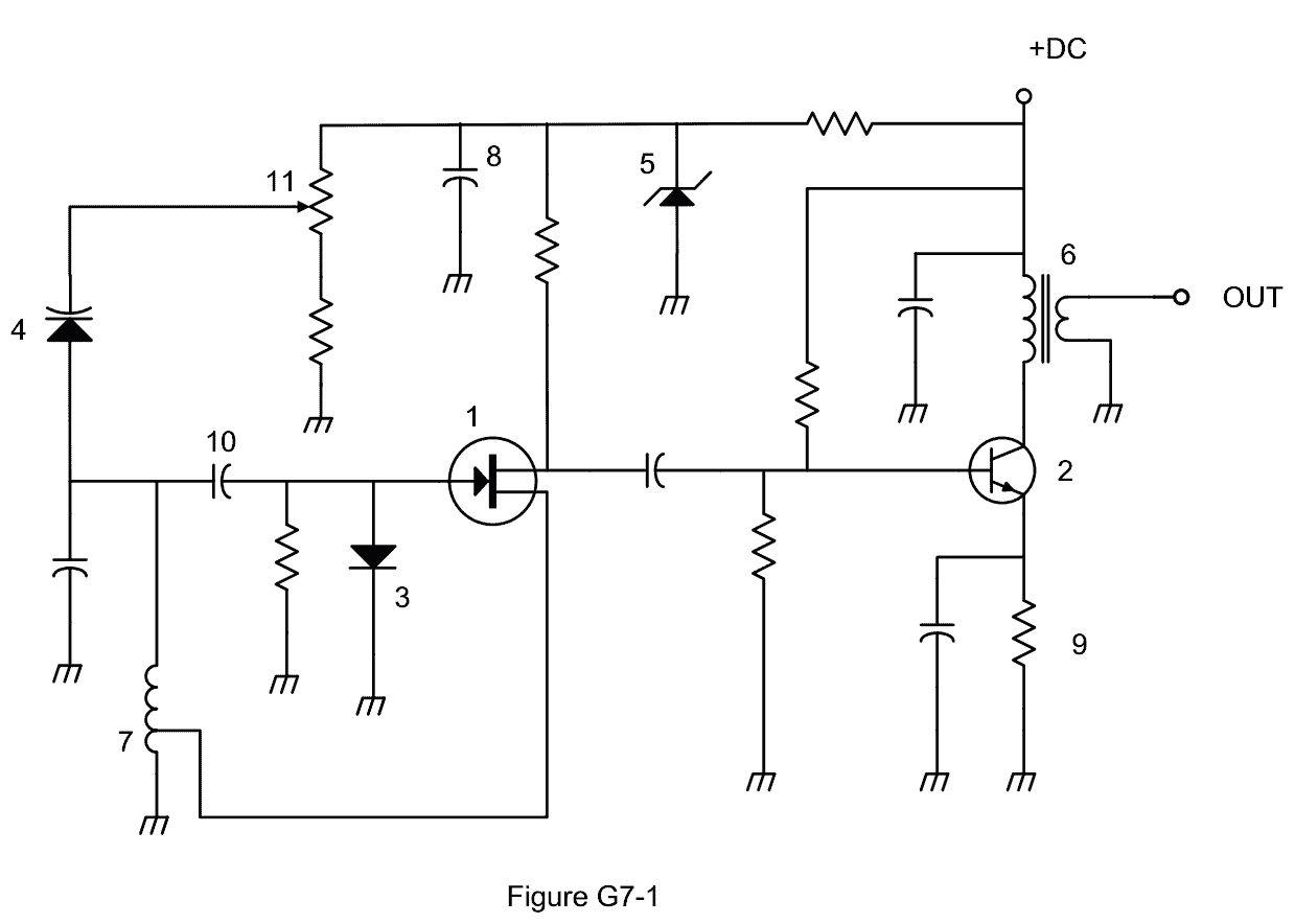
Link to circuit symbol guide: [Wikipedia Gallery of Common Electronic Symbols] (http://en.wikipedia.org/wiki/Electronic_symbol#Gallery_of_common_electronic_s ymbols)
Hint: The question and answer both have power.
Last edited by donaldbush. Register to edit
Tags: none
Which of the following components are used in a power-supply filter network?
-
Diodes
-
Transformers and transducers
-
Quartz crystals
-
Correct AnswerCapacitors and inductors
Both capacitors and inductors are FILTERS and are used in a power-supply filter network. The combination of these two components is often referred to as an LC circuit (L is the Inductor, C is the Capacitor). Together they act to "tune" the circuit to smooth out voltage and current pulses from the power supply to provide a constant DC output voltage.
For more info see Wikipedia: LC circuit
Last edited by ironcal67. Register to edit
Tags: none
What is the peak-inverse-voltage across the rectifiers in a full-wave bridge power supply?
-
One-quarter the normal output voltage of the power supply
-
Half the normal output voltage of the power supply
-
Double the normal peak output voltage of the power supply
-
Correct AnswerEqual to the normal peak output voltage of the power supply
(D) The Peak-inverse-voltage across the rectifiers in a full-wave bridge power supply is EQUAL to the normal peak output voltage of the power supply. Diodes and rectifier diodes are not constructed to run in reverse flow patterns. The maximum voltage that they can handle in the reverse direction without being damaged or destroyed is the peak-inverse voltage. In a full-wave bridge power supply circuit, the amount of voltage that would be sent backwards is equal to the normal peak output voltage of the power supply.
Hint: An easy way to remember for a full-wave bridge is that a full wave = 1 or (1) / (1), if you reverse the fraction as you would reverse the current flow, you still get (1) / (1), or the system is equal.
For more info see Wikipedia: Peak-inverse voltage, Rectifier
Last edited by heroiclemon. Register to edit
Tags: none
What is the peak-inverse-voltage across the rectifier in a half-wave power supply?
-
One-half the normal peak output voltage of the power supply
-
One-half the normal output voltage of the power supply
-
Equal to the normal output voltage of the power supply
-
Correct AnswerTwo times the normal peak output voltage of the power supply
(D). The peak-inverse-voltage across the rectifier in a half-wave power supply is TWO times the normal peak output voltage of the power supply. The peak- inverse voltage is the amount of voltage that the diode or diode rectifier can withstand in the reverse flow direction, without being damaged or destroyed. In the case of a half-wave power supply, the amount of voltage being reversed that the diode must cope with is full peak voltage from the capacitor plus a value of the peak voltage (in the opposite polarity) from the transformer.
Hint: An easy way to remember is that for a 1/2 wave power supply, reverse the fraction as you would reverse the voltage, so change (1) / (2) forward to (2) / (1) reversed = 2.
The question is a little misleading.
Without a filter, during negative half cycle of input voltage, the diode is reverse biased. There is no current flow to the load, so voltage across the load is zero. Hence the complete input voltage is across the diode, so PIV = input voltage, Vp
However the question apparently assumes a half wave rectifier WITH a capacitor filter. Here, the capacitor is connected across the load. During positive half cycle of input voltage, that capacitor is charged to Vp. During negative half cycle of input voltage (diode is reverse biased) , the capacitor is discharged to the load, from Vp. Hence considering the maximum voltage across diode during reverse biased condition, diode anode voltage = -Vp, since negative half cycle. Diode cathode voltage = +Vp. Diode voltage during reverse bias = Vp--Vp = 2Vp.
For more info see Wikipedia: Peak-inverse voltage, Rectifier
Last edited by korky. Register to edit
Tags: none
What portion of the AC cycle is converted to DC by a half-wave rectifier?
-
90 degrees
-
Correct Answer180 degrees
-
270 degrees
-
360 degrees
(B). A half-wave rectifier will convert 1/2 of the full AC cycle of 360 degrees, so it will convert 180 degrees of the wave to DC.
For more info see Wikipedia: Rectifier
Last edited by kd7bbc. Register to edit
Tags: none
What portion of the AC cycle is converted to DC by a full-wave rectifier?
-
90 degrees
-
180 degrees
-
270 degrees
-
Correct Answer360 degrees
A FUll-wave = \(360°\)
As its name indicates, a full-wave rectifier will convert the full wave or 360 degrees of the AC waveform to DC.
A half-wave rectifier converts only half of the waveform, and is 180 degrees of the input sine wave.
Hint: Think "going full-circle" - all 360 degrees.
For more info see Wikipedia: Rectifier
Last edited by unclepop16. Register to edit
Tags: none
What is the output waveform of an unfiltered full-wave rectifier connected to a resistive load?
-
Correct AnswerA series of DC pulses at twice the frequency of the AC input
-
A series of DC pulses at the same frequency as the AC input
-
A sine wave at half the frequency of the AC input
-
A steady DC voltage
Hint: a full wave rectifier is TWICE the fun.
The output waveform of an unfiltered full-wave rectifier connected to a resistive load will be a series of DC pulses at twice the frequency of the AC input. The rectifier will change each half cycle of the AC current waveform into pulses of DC current. This results in one pulse for the positive 1/2 cycle and one pulse for the negative 1/2 cycle for a total of 2 pulses DC output for each wavelength of AC converted.
For more info see Wikipedia: Rectifier
Last edited by gconklin. Register to edit
Tags: none
Which of the following is an advantage of a switch-mode power supply as compared to a linear power supply?
-
Faster switching time makes higher output voltage possible
-
Fewer circuit components are required
-
Correct AnswerHigh frequency operation allows the use of smaller components
-
All of these choices are correct
Hint: a Switchmode uses SMALLER components, NOT FEWER.
An advantage of a switch mode power supply over a linear power supply, is that the high frequency operation allows the use of smaller components. This type of power supply is highly efficient and switches very quickly. The high operating frequencies (typically 50 kHz - 1 MHz instead of much lower 60 Hz AC) means that compact and lightweight transformers can be used. This makes a great difference in the size and weight of the equipment.
For more info see Wikipedia: Switched-mode power supply
Last edited by gconklin. Register to edit
Tags: none
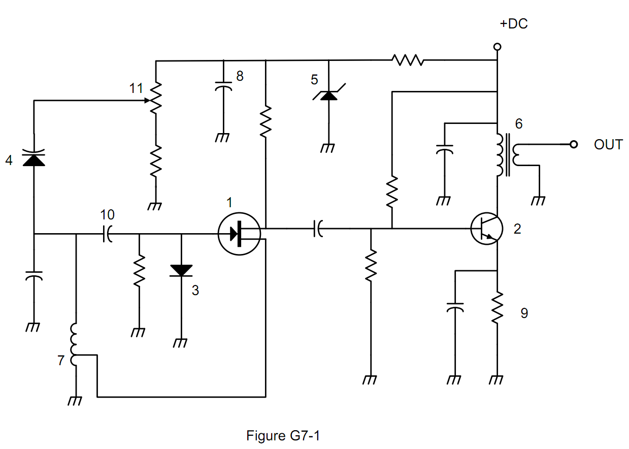
Which symbol in figure G7-1 represents a field effect transistor?
-
Symbol 2
-
Symbol 5
-
Correct AnswerSymbol 1
-
Symbol 4
Symbol 1 in figure G7-1 represents a field effect transistor.
The figure shows the arrow coming IN from the GATE to meet the vertical bar, representing the transistor, at center left. At the top of the bar the upper terminal has a perpendicular line to the right indicating the DRAIN. While at the bottom of the bar the lower terminal has a perpendicular line to the right indicating the SOURCE.
Link to circuit symbol guide: Wikipedia Gallery of Common Electronic Symbols
For more info see Wikipedia: Field effect transistor
Last edited by kd7bbc. Register to edit
Tags: none

Which symbol in figure G7-1 represents a Zener diode?
-
Symbol 4
-
Symbol 1
-
Symbol 11
-
Correct AnswerSymbol 5
(D). Symbol 5 represents a Zener diode.
The figure is represented by a horizonal bar across the vertical circuit line. The left end of this bar tilts down, and the right end tilts up. These tilts represent the change in voltage beween the input and output. These tilts make it look a little like a Z on its side - as a reminder for "Zener." Pointing into the bottom center of the horizontal bar is a triangle, located on the circuit line and the tip hitting the bar. This triangle symbol represents the voltage drop, D, of the diode.
Note for the visually impaired: If possible, notify your VE in advance of any accommodation you may need. They may be able to give you an exam without questions on figure G7-1. A worded description of the symbol is given here for both your own knowledge and to be able to describe the symbol to the VE if necessary.
Refer to the following links for the official exam circuit figure and symbol guide:
Figure G7-1 (.jpg format): http://www.ncvec.org/downloads/Revised%20G7-1.jpg
Figure G7-1 (.pdf format): http://www.ncvec.org/downloads/Revised%20G7-1.pdf
Link to circuit symbol guide: Wikipedia Gallery of Common Electronic Symbols
For more info see Wikipedia: Zener diode
Last edited by qubit. Register to edit
Tags: none

Which symbol in figure G7-1 represents an NPN junction transistor?
-
Symbol 1
-
Correct AnswerSymbol 2
-
Symbol 7
-
Symbol 11
Symbol 2 represents an NPN junction transistor. A common way to remember the symbol for an NPN transistor is that the arrow is Not Pointing iN.
The transistor is represented by a vertical bar with a line coming in to the center of the bar from the left (Base). The upper terminal has a line coming into the right at an upward 45 degree angle (Collector). The lower terminal has a line to the right downward 45 degree angle (Emitter) with an arrow pointing away from the transistor.
Note for the visually impaired:
If possible, notify your VE in advance of any accommodation you may need. They may be able to give you an exam without questions on figure G7-1. A worded description of the symbol is given here for both your own knowledge and to be able to describe the symbol to the VE if necessary.
Refer to the following links for the official exam circuit figure and symbol guide:
Link to circuit symbol guide: Wikipedia Gallery of Common Electronic Symbols
For more info see Wikipedia: NPN or Bipolar junction transistor
Last edited by kd7bbc. Register to edit
Tags: none

Which symbol in Figure G7-1 represents a multiple-winding transformer?
-
Symbol 4
-
Symbol 7
-
Correct AnswerSymbol 6
-
Symbol 1
(C). Symbol 6 represents a multiple-winding transformer.
The core of the transformer is represented by two long vertical parallel lines close together (if there were no lines, the core would be air). On the left side of the core is the primary winding represented as vertical line with multiple connected semi-circular dips or waves, with the bottoms of the waves towards the core, and the pointed wave peaks pointing away from the core. On the right side is the secondary winding represented by a similar wavy line (bottoms of the waves toward the core). The number of windings on the two sides can be the same or different (which would indicate a step-up or step-down transformer). The symbol shown in figure G7-1 shows 4 windings on the left and 2 on the right.)
Refer to the following links for the official exam circuit figure and symbol guide:
Figure G7-1 (.jpg format) (result: 404 Error Message)
Figure G7-1 (.pdf format) (result: 404 Error Message)
Link to circuit symbol guide: Wikipedia Gallery of Common Electronic Symbols
For more info see Wikipedia: Multiple-winding transformer
Last edited by zayaan.raeid. Register to edit
Tags: none

Which symbol in Figure G7-1 represents a tapped inductor?
-
Correct AnswerSymbol 7
-
Symbol 11
-
Symbol 6
-
Symbol 1
An inductor is a coil; symbol 7 is mostly the same symbol as a normal inductor, which is intended to represent that coil. (note symbol 6 as well which is a transformer, which consists of two coils).
A tapped inductor is one in which it's possible to "tap" a point in the coil to effectively shorten the coil. Sometimes that tap can be moved. Thus the symbol shows a wire coming off of the side of the coil in the symbol, indicating the tap.
Last edited by ironcal67. Register to edit
Tags: none
View Privacy Policy | Get help with HamStudy.org™
