PRACTICAL CIRCUITS
Active filters and op-amps: active audio filters; characteristics; basic circuit design; operational amplifiers
What primarily determines the gain and frequency characteristics of an op-amp RC active filter?
-
The values of capacitors and resistors built into the op-amp
-
Correct AnswerThe values of capacitors and resistors external to the op-amp
-
The input voltage and frequency of the op-amp's DC power supply
-
The output voltage and smoothness of the op-amp's DC power supply
Tags: none
What is the effect of ringing in a filter?
-
An echo caused by a long time delay
-
A reduction in high frequency response
-
Partial cancellation of the signal over a range of frequencies
-
Correct AnswerUndesired oscillations added to the desired signal
Ringing simply means that part of your circuit is at resonance and oscillating (like a bell). In some cases this is good - without oscillators there would be no CW! In other cases however, the ringing interferes with the function of the circuit. In this case, the filter is adding its own component to the output signal. This can sometimes be heard as a tone or whistle over the desired audio.
REMEMBER: Ringing is Undesired
Last edited by w9mpx. Register to edit
Tags: none
Which of the following is an advantage of using an op-amp instead of LC elements in an audio filter?
-
Op-amps are more rugged
-
Op-amps are fixed at one frequency
-
Op-amps are available in more varieties than are LC elements
-
Correct AnswerOp-amps exhibit gain rather than insertion loss
Ideally, capacitors and inductors only store energy, and do not have any losses. However, real devices do present losses (e.g. material resistance, and heat), and since they are passive, they cannot increase the energy in the circuit in any way. This is called insertion loss.
On the other hand, an op amp is an active device (connected to the power source). Energy losses are accounted to the power source, not to the processed signal.
Last edited by robotoloco. Register to edit
Tags: none
Which of the following is a type of capacitor best suited for use in high-stability op-amp RC active filter circuits?
-
Electrolytic
-
Disc ceramic
-
Correct AnswerPolystyrene
-
Paper
The capacitor dielectric material between the two electrodes is what's being described here.
The keyword "high-stability" refers to low temperature dependence and long life time. According to wikipedia--plastics offer better stability and ageing performance, and polystyrene is the only plastic in the answers.
Last edited by xyzhangj. Register to edit
Tags: none
How can unwanted ringing and audio instability be prevented in a multi-section op-amp RC audio filter circuit?
-
Correct AnswerRestrict both gain and Q
-
Restrict gain, but increase Q
-
Restrict Q, but increase gain
-
Increase both gain and Q
To prevent ringing and audio instability in an op-amp audio filter, you should restrict both gain and Q.
- Q (quality factor) determines how "sharp" or selective a filter is. A high Q can cause peaking in the frequency response, which can lead to oscillation or ringing.
- Gain in the feedback loop can amplify small disturbances, making instability worse.
By limiting both the gain and the Q, you reduce the likelihood of the filter becoming unstable or producing unwanted oscillations.
Mneumonic: To keep audio true, restrict gain and Q
Last edited by km4ckd. Register to edit
Tags: none
Which of the following is the most appropriate use of an op-amp active filter?
-
As a high-pass filter used to block RFI at the input to receivers
-
As a low-pass filter used between a transmitter and a transmission line
-
For smoothing power-supply output
-
Correct AnswerAs an audio filter in a receiver
In the 4 answers, only 3 are filters (contain the word filter). We know that a perfect (theoretical) op-amp would have a flat response so this is neither a low-pass or a high-pass.
We are left with the correct answer: As an audio filter in a receiver.
-chevdor
Last edited by ke0ipr. Register to edit
Tags: none

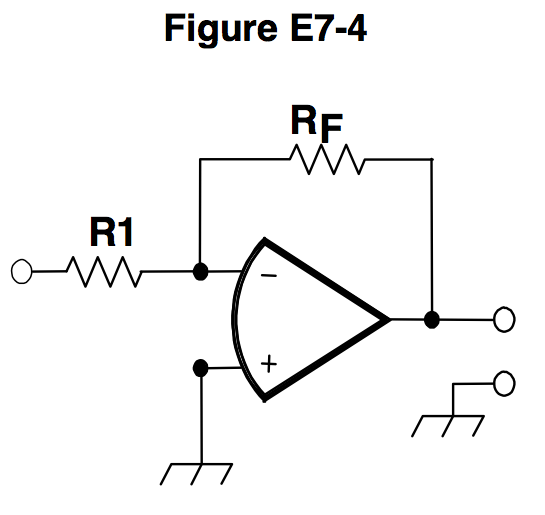
What magnitude of voltage gain can be expected from the circuit in Figure E7-4 when R1 is 10 ohms and RF is 470 ohms?
-
0.21
-
94
-
Correct Answer47
-
24
By the voltage gain formula where \(A\) represents the operational amplifier (op-amp) voltage gain,
\begin{align} A_{\text{voltage}}&=\frac{V_\text{out}}{V_\text{in}}=-\frac{R_F}{R_1}=-\frac{470\:\Omega}{10\:\Omega}\\ &=-47 \end{align}
The magnitude is all that is required, so \(\mid A_{\text{voltage}}\mid=47\) is the answer.
Applying the ideal operational amplifier constraints we can determine circuit behavior.
Infinite gain implies zero difference between the inputs at steady state. Therefore the node at the inverting(-) input will be ground or 0 V. (a)
Infinite input impedance means that all current that flows through \(R1\) must flow out through \(R_F\). (b)
Putting (a) and (b) together for an input voltage V, will induce a current in R1 which is \(I = \frac{(V_{\text{in}}-0)}{R1}\), which must equal the current in \(R_F\) which is \(I = \frac{(0-V_{\text{out}})}{R_F}\).
From this, \(\frac{V_{\text{in}}}{R1} = -\frac{V_{\text{out}}}{R_F}\). Rearranging by multiply everything by \(R_F\) and dividing everything by \(V_{\text{in}}\) to get \(\frac{R_F}{R1} = -\frac{V_{\text{out}}}{V_{\text{in}}}\). Therefore in this configuration the gain is \(-\frac{R_F}{R1}\) which is \(-\frac{470\:\Omega}{10\:\Omega}\) or \(-47\). Again, because the only the magnitude is requested, the negative sign can be dropped.
HINT: In the Schematic diagram the RF is over the R1. Think of RF divided by R1 (RF/R1).
Last edited by bsolov. Register to edit
Tags: none
How does the gain of an ideal operational amplifier vary with frequency?
-
It increases linearly with increasing frequency
-
It decreases linearly with increasing frequency
-
It decreases logarithmically with increasing frequency
-
Correct AnswerIt does not vary with frequency
Ideal operational amplifiers can be found at your local physics store, right next to frictionless surfaces and massless springs...
They don't really exist!
If they did, they would have infinite input impedance (draw no current), zero output impedance, no offset, stable at all gains, and have flat frequency response from DC to Cosmic Rays...
When analyzing the behavior of an op-amp circuit, it is often useful to start with looking at it with an ideal op-amp in place to understand its theoretical "best" behavior. Included with that is the fact that an ideal op-amp does not have frequency-dependent gain.
Study hint: Ideal operational amplifier does not exist 'does not' is in only 1 answer.
Last edited by thepctech. Register to edit
Tags: none

What will be the output voltage of the circuit shown in Figure E7-4 if R1 is 1000 ohms, RF is 10,000 ohms, and 0.23 volts dc is applied to the input?
-
0.23 volts
-
2.3 volts
-
-0.23 volts
-
Correct Answer-2.3 volts
This schematic is of a simple one-stage inverting op-amp amplifier.
The gain, G, is defined as:
\[G = \frac{-R_\text{F}}{R_\text{in}}\]
Where:
\(R_\text{F}\) is the "feedback resistor" and
\(R_\text{in}\) is the "input resistor" (R1 in our
diagram).
\[G=\frac{-R_\text{F}}{{R1}}=\frac{-10000\:\Omega}{1000\:\Omega}=-10\]
The output voltage is the gain multiplied by the input voltage. Therefore, \[0.23\:\text{V} \times -10 = -2.3\:\text{V} \]
Explanation for the negative sign in the gain equation: The gain here is 10 times the input voltage, but the input is applied to the inverting(-) input of the amplifier and RF from the output to the inverting(-) input to generate negative feedback to limit gain, making the voltage gain -10.
Another way to think about it is that with negative feedback, the opamp will try to make the two inputs equal, so the feedback will be \(0V\). If there is a voltage divider of \(R1\) and \(R_F\) with \(.23V\) on one side and the middle is \(0V\), the far end of the divider needs to be \(-2.3V\); \(R1\) must drop \(.23V\), so Rf must drop \(10\times\) the voltage. Since \(IR1=IR_F\), \(\frac{Vin-0V}{R1} = \frac{0-V_\text{out}}{R_F}\); \(V_\text{out} = \frac{-R_F}{R1} \times V_\text{in} = -2.3V\)
Last edited by gregor. Register to edit
Tags: none

What absolute voltage gain can be expected from the circuit in Figure E7-4 when R1 is 1800 ohms and RF is 68 kilohms?
-
1
-
0.03
-
Correct Answer38
-
76
This schematic is of a simple one-stage inverting op-amp amplifier.
The gain, G, is defined as:
\[G = \frac{-R_\text{F}}{R_\text{in}}\]
Where:
\(R_\text{F}\) is the "feedback resistor" and
\(R_\text{in}\) is the "input resistor" (R1 in our
diagram).
The gain is negative because the inverting input is used. So, for this question:
\begin{align}
R_\text{in} = R1 &= 1800\:\Omega \\
R_\text{F} = 68\:\text{k}\Omega &= 68000\:\Omega
\end{align}
Therefore the gain is: \(G = \frac{-68000\:Ω}{1800\:Ω} = -37.7\)
The question asks for absolute voltage gain, so the sign of the answer is eliminated:
\[\left| G\right| =37.7777...\approx38\]
Test trick: To remember the formula, note that in the diagram, the \(R_\text{F}\) is 'over' the \(R_\text{1}\).
HINT: There are many number "8" in the question ... and correct answer.
Last edited by herve205. Register to edit
Tags: none

What absolute voltage gain can be expected from the circuit in Figure E7-4 when R1 is 3300 ohms and RF is 47 kilohms?
-
28
-
Correct Answer14
-
7
-
0.07
The gain, G, is defined as:
\[G = \frac{R_\text{F}}{R_\text{in}}\]
Where:
\(R_\text{F}\) is the "feedback resistor" and
\(R_\text{in}\) is the "input resistor" (R1 in our
diagram).
The absolute voltage gain that can be expected from the circuit in Figure E7-3 when R1 is 3300 ohms and \(R_\text{F}\) is 47 kilohms is:
\[G = \frac{47,000\:Ω}{3,300\:Ω} =14.2424...\approx14\]
Tip: Note that in the diagram, \(R_\text{F}\) is over R1, which gives you a hint of how to work the formula.
Hint: There are 4's in both the question and the answer. The answer has the only duplicated number from the question.
Last edited by yr7 - extra. Register to edit
Tags: none
What is an integrated circuit operational amplifier?
-
Correct AnswerA high-gain, direct-coupled differential amplifier with very high input and very low output impedance
-
A digital audio amplifier whose characteristics are determined by components external to the amplifier
-
An amplifier used to increase the average output of frequency modulated amateur signals to the legal limit
-
An RF amplifier used in the UHF and microwave regions
An operational amplifier (op-amp) is a DC-coupled high-gain electronic voltage amplifier with a differential input and, usually, a single-ended output. In this configuration, an op-amp produces an output potential (relative to circuit ground) that is typically hundreds of thousands of times larger than the potential difference between its input terminals. Its input impedance is very high and its output impedance is very low. (From Wikipedia)
HINT: I would search HIGH and LOW for a good OPERATIONAL AMPLIFIER.
Last edited by yr7 - extra. Register to edit
Tags: none
What is meant by the term op-amp input-offset voltage?
-
The output voltage of the op-amp minus its input voltage
-
The difference between the output voltage of the op-amp and the input voltage required in the immediately following stage
-
Correct AnswerThe differential input voltage needed to bring the open-loop output voltage to zero
-
The potential between the amplifier input terminals of the op-amp in an open-loop condition
An op-amp is DC powered and when simply connected and powered-up with no other components the output will contain a DC bias. However, applying an input voltage will result in it being amplified and combined with the DC bias leaving a new output voltage.
Because the op-amp will amplify a positive or negative voltage, it is possible to choose a specific input voltage that results in the combined amplified and bias voltage at the output equaling zero volts. This input voltage that leads to a zero volt output with no other circuitry is known as the input-offset voltage.
Hint: The correct answer has the words "Differential & zero ".
Hint: Think about a scale. If it is "off-set" you try to get the scale to show zero when nothing is on it. (This is not just with a scale, lots of things are "off-set" from zero). In this case the answer has zero, and the question is talking about input offset voltage.
Last edited by gregor. Register to edit
Tags: none
What is the typical input impedance of an integrated circuit op-amp?
-
100 ohms
-
1000 ohms
-
Very low
-
Correct AnswerVery high
Tags: none
What is the typical output impedance of an integrated circuit op-amp?
-
Correct AnswerVery low
-
Very high
-
100 ohms
-
1000 ohms
A theoretical op-amp (operational amplifier) is the ideal voltage amplifier, with infinite input impedance and zero output impedance (in real devices, change "infinite" and "zero" to "very high" and "very low").
Very high input impedances create light loads, as the current is small through them. This means that the op-amp does not load its driver circuit.
With very low output impedances, all the voltage drop occurs in the load (picture an equivalent circuit with the output impedance in series with the load). This means that almost all of the voltage amplification is delivered to the load, which is a nice feature to have in an amplifier.
MEMORY HINT:
- Think - (I)nput pointing to Very h(i)gh
- Think - (O)utput pointing to Very l(o)w
SILLY HINT: Think OIL: Output Impedance Low
Last edited by gregor. Register to edit
Tags: none
View Privacy Policy | Get help with HamStudy.org™
